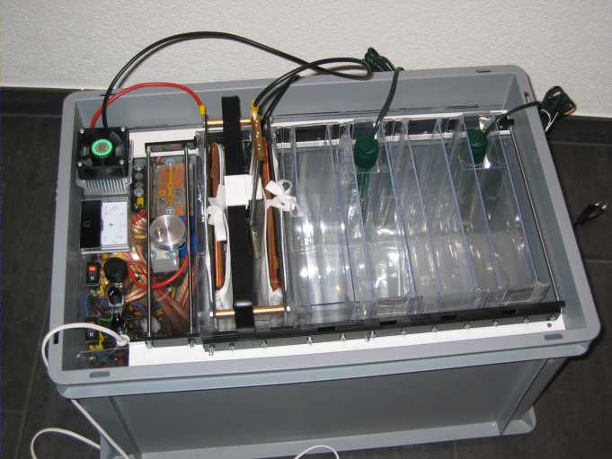

I got sick of waiting for my PCB's to be made externaly and therefore wanted to be able to produce PCB's for my prototypting needs by myself. Now, it is not too difficult to create even double sided PCB's at home. However, having the vias conect the two layers by hand is a real pain. More advanced layouts also can't be made with doulbe sided PCB's and that's then usually the end of the rope when it comes to homebrew PCB's.
Unless you have a through plating station of course!
Haveing such a machine put's you in the position to create real multilayer PCB's on your own - something I was dreaming of for long.
This page is intended to give you ideas on how to build your own station.
The ongoing changes to the station are documented here: Updates to the station
The ideas behind the TPS were:
The station is safe to operate if it is mechanically stable, if all options can be turned on and off individually, if the PCB is easy to put from one tank into the next one etc.
Protection against leakage - that's actually the thing I was most afraid of - is reached due to the fact that the main box is made of plastics. That said, if a tank leakes, nothing can really leave the station. Then, the station is of course having a main fuse and most importantly shall not be plugged in if not in use!
For those of you being afraid that the electronics could be contaminated, the pictures maybe don't show this good enough, but all the electronics are mounted at a hight in the box where THREE TANKS could leak at the same time and no chemicals would reach either the main transformer nor the PCB holding the simple electronics needed.
Serviceability was important to me too. The whole station can be put apart in only one minute! This makes it really easy to change things, clean the station if the need arises, or take apropriate quick actions in case a leakeage ocures. In other words, the serviceability is also important with regard to the save operation of the station. See Put into parts for a picuture of the individual parts of the station.
Some closeups and bigger variants of the images of the station. WARNING!!! Some of the pictures are huge!
Don't forget that there are no warranties associated with information presented on these pages. I of course try hard to give as apropriate information I can and also to inprove the station where needed. I'm however in no way responsible if the station does not work the way you would expect it to work. If it burns your house, blows up your city or does any other harmful thing to you or any other party - it is entirely your problem. I am not liable for any infringements or damages of third parties' rights resulting in your use of this product. I am not liable for, and do not warrant the trustworthiness, quality, industrial use, or serviceability of this product for the supposed purpose or any other purposes.
| file: /Techref/pcb/plating/tps-overview.htm, 5KB, , updated: 2018/3/23 15:21, local time: 2025/4/28 10:51,
18.118.155.106:LOG IN
|
| ©2025 These pages are served without commercial sponsorship. (No popup ads, etc...).Bandwidth abuse increases hosting cost forcing sponsorship or shutdown. This server aggressively defends against automated copying for any reason including offline viewing, duplication, etc... Please respect this requirement and DO NOT RIP THIS SITE. Questions? <A HREF="http://linistepper.com/Techref/pcb/plating/tps-overview.htm"> Homebrew Through Hole PCB Plating Station - Overview</A> |
| Did you find what you needed? |